

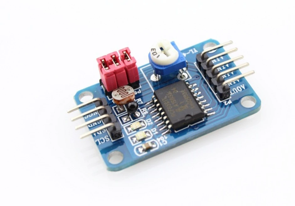
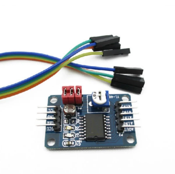
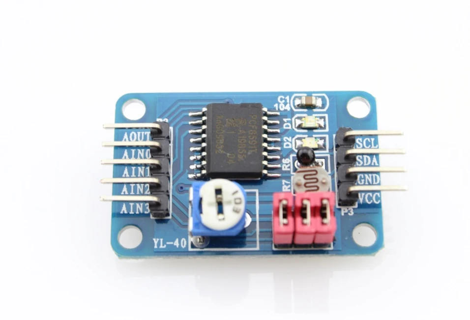
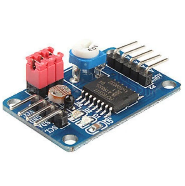
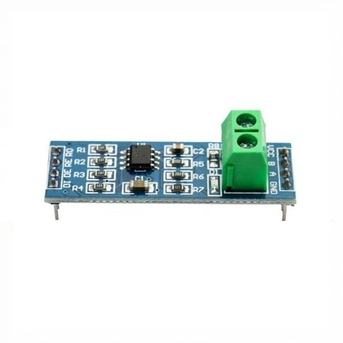
This is a breakout board/Prototype Board for PCF8591 IC. The PCF8591 Module Analog to Digital / Digital-Analog Converter Module with F-F Jumper Wire is a single-chip, single‑supply low‑power 8‑bit CMOS data acquisition device with four analog inputs, one analog output, and a serial I²C‑bus interface. Three address pins A0, A1, and A2 are used for programming the hardware address, allowing the use of up to eight devices connected to the I²C‑bus without additional hardware. Address, control, and data to and from the device are transferred serially via the two-line bidirectional I²C‑bus.
The functions of the device include analog input multiplexing, on-chip track and hold function, 8-bit analog‑to‑digital conversion, and an 8‑bit digital‑to‑analog conversion. The maximum conversion rate is given by the maximum speed of the I²C-bus.
| Operating Voltage (VDC) | 2.5 to 6 |
|---|---|
| IC Chip | PCF8951 |
| PCB Size ( L x W ) mm | 35 x 23 |
| Shipping Weight | 0.06 kg |
| Shipping Dimensions | 8 × 7 × 3 cm |
1 x PCF8591 Module Analog to Digital / Digital-Analog converter module with F-F Jumper Wire
No review given yet!
 Fast Delivery all across the country
 Safe Payment
 7 Days Return Policy
 100% Authentic Products


You need to Sign in to view this feature
This address will be removed from this list